
Research
Interpretable AI and robotics for physics
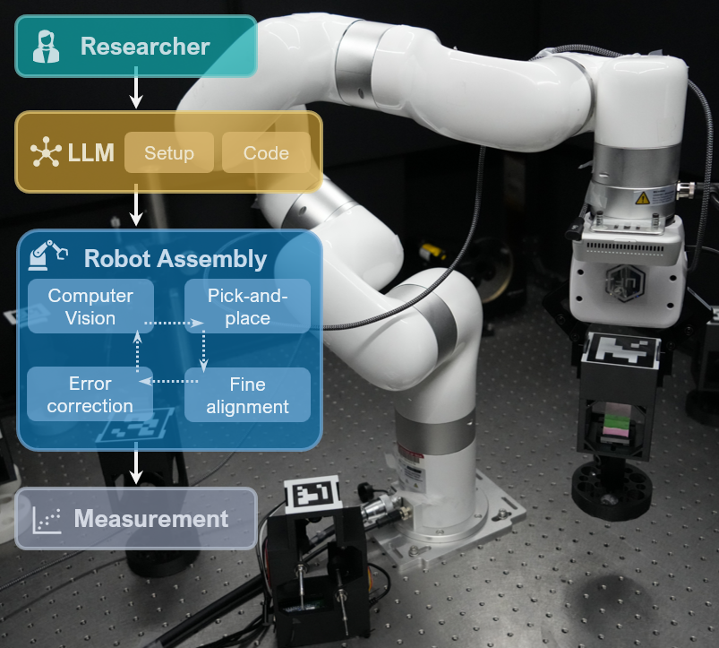
Current AI models, while capable of achieving high accuracies in various tasks, are fundamentally limited in terms of interpretability. Advancements in physics often rely on key insights derived from theoretical developments, experimental observations or numerical simulations. Consequently, developing novel AI frameworks that align closely with scientific goals is crucial for leveraging AI's capabilities for fundamental discoveries. Furthermore, as developments in AI continue to advance rapidly, there is a growing need to integrate robotic solutions with AI for accelerating experimental science through automation and intelligent decision-making.
Some key questions that inform my research:
- How do we develop interpretable AI models that are closely aligned with scientific goals?
- What does a future that employs robotics and AI for physics experiments look like?
References:
[1] KAN: Kolmogorov-Arnold Networks, ICLR (2025)
[2] AI-Driven Robotics for Optics, arXiv:2505.17985 (2025)
[3] Symbolic Learning of Topological Bands in Photonic Crystals, arXiv:2505.10485 (2025)
[4] Gradient-Based Search of Quantum Phases: Discovering Unconventional Fractional Chern Insulators, arXiv:2509.10438 (2025)
[5] Refining Heuristic Predictors of Fractional Chern Insulators using Machine Learning, arXiv:2512.01873 (2025)
Nanophotonics

The field of nanophotonics focuses on the manipulation and control of light on the nanometer scale. The unique properties of light-matter interactions at these scales arise from the confinement of photons to dimensions comparable to the wavelength of light. This confinement leads to phenomena such as enhanced optical transport, strong light-matter coupling, and the ability to manipulate light in ways that are impossible with traditional optical components. This precise control makes it possible to leverage phenomena like the Purcell effect to increase spontaneous emission rates or supercollimation to guide light.
Some key questions that inform my research:
- Can we find novel strategies for trapping and guiding light at the nanoscale?
- What new functionalities can be achieved by leveraging nanophotonics for scintillation?
References:
[1] Tunable Nanophotonic Devices and Cavities based on a Two-Dimensional Magnet, Nature Photonics 19, 1006–1012 (2025)
[2] Reentrant delocalization transition in one-dimensional photonic quasicrystals, Physical Review Research 5, 033170 (2023)
[3] Observation of Bound States in the Continuum Embedded in Symmetry Bandgaps, Science Advances 7, 52 eabk1117 (2021)
[4] Point-Defect-Localized Bound States in the Continuum in Photonic Crystals and Structured Fibers, Physical Review Letters 127, 023605 (2021)
Topological quantum matter
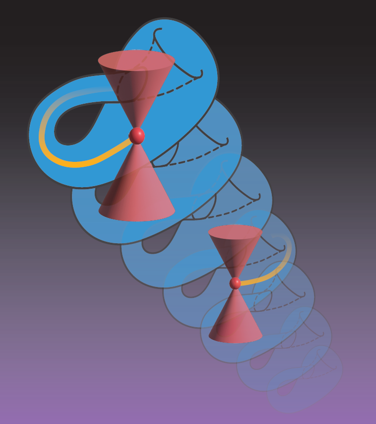
Topological insulators and semimetals are fascinating classes of materials that have recently emerged as a prominent subject of study in condensed matter physics. They represent new phases of matter that possess unique properties at their surfaces, hinges, edges or corners, distinct from those in the bulk. This results ultimately from the underlying non-trivial topology of the electronic band structure rather than any specific material property. Moreover, when quasiparticle interactions are strong, topological phases of matter can give rise to even more exotic phenomena, such as fractionalization and topological order. In the last decade, many ideas from topological matter have been extended to other systems that host wave-like excitations, such as light propagating in photonic crystals, where they serve as new guiding principles for design.
These are some key questions that inform my research:
- What novel phases of matter arise from the interplay of symmetry, geometry, and topology?
- How can we robustly control noise and excitations in quantum systems using topological principles?
References:
[1] Noise Immunity in Quantum Optical Systems through Non-Hermitian Topology, arXiv:2503.11620 (2025)
[2] Quantized Crystalline-Electromagnetic Responses in Insulators, Physical Review Letters 135, 256602 (2025)
[3] Weyl Points on Non-Orientable Manifolds, Physical Review Letters 132, 266601 (2024)
[4] Polarization and Weak Topology in Chern Insulators, Physical Review Letters 132, 116602 (2024)
[5] Observation of a Charge-2 Photonic Weyl Point in the Infrared, Physical Review Letters 125, 253902 (2020)